(a) Define doping (1mk)
Process of introducing foreign element (impurity) into a pure semi-conductor,
(b) Distinguish between a p-type and n-type semi conductors (2mks)
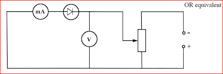
(c) Using a diagram illustrate a forward P-N junction (2mks)(d) The figure below shows a bridge circuit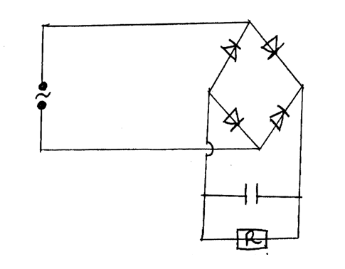
A capacitor has been connected across the resistor as shown
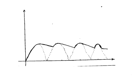
(i) Sketch of the figure below the wave form when a CRO is connected across the resistor, R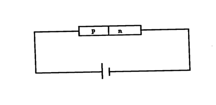
(ii) On the same axes, sketch a wave form when C.R.O is connected across R when the capacitor has been removed (1mk)
0 Comments
K.C.S.E Physics Q & A - MODEL 2018PP2QN18
(a) (i) Draw a circuit diagram showing the depletion layer of a p—n junction diode connected in the reverse bias mode.
(ii) State the reason why increasing the external voltage in (i) makes the depletion layer wider. (iii) State the meaning of breakdown voltage of a junction diode. (iv) State one application of diodes. (b) Figure 7 shows the output on a screen of a CR0 when an a.c. signal is connected to the Y-plates with the time base on. 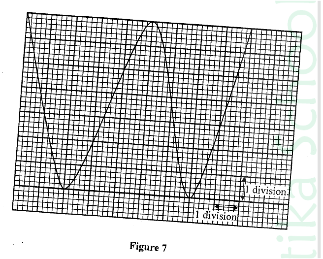
(i) Given that the time control is 5 ms per division and the y-gain is 100 V per division determine the:
(I) frequency of the ac. signal (II) peak voltage of the input signal (ii) State the adjustment that may be made in order to halve the frequency of the a.c. signal.
answers
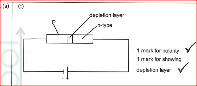
(ii) The holes and the electrons in their respective regions are attracted away from the junction by the external voltage.
(iii) The voltage at which the diode begins to conduct in the reverse bias mode. (iv) In rectification circuits for changing a.c. to d. c. In control of voltages of Zener diode. 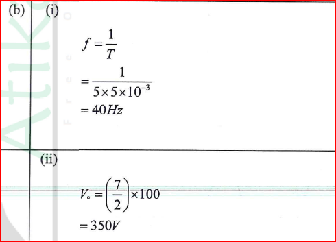
(iii) Double the time control to 10ms per division.
Adjust the frequency of the source to half the value K.C.S.E Physics Q & A - MODEL 2018PP2QN09
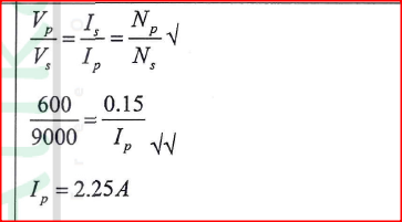
A transformer has 600 turns in the primary coil and 9000 turns in the secondary coil. The transformer is 100% efficient and the current in the secondary coil is 0.15A, determine current in the primary coil.

answer
K.C.S.E Physics Q & A - MODEL 2017PP2QN17
(a) Figure 8 shows a conductor AB connected to a galvanometer and placed between two permanent magnets.
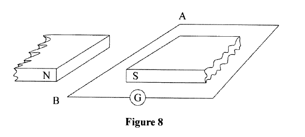
(i) Conductor AB is moved perpendicular to the magnetic field.
State and explain the observation made on the galvanometer. (ii) State the effect of moving the conductor faster. (b) A transformer is used to step down 240V to 12 V for use in an electric appliance operating at 0.5 A. If the primary coil has 600 turns, determine the; (i) number of turns ¡n the secondary coil, (ii) current in the primary coil.
answers
a) i. A momentary deflection is observed, Conductor cuts the field.
An emf is induced in AB Causing current in the circuit ii. A bigger deflection is observed! higher current 
K.C.S.E Physics Q & A - MODEL 2017PP2QN08
Draw a circuit diagram to show a p-n junction diode in the forward biased mode.
answer
K.C.S.E Physics Q & A - MODEL 2016PP2QN17
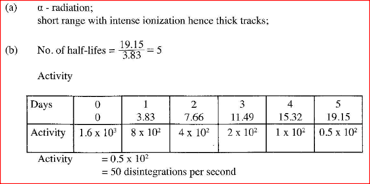
When a radiation was released into a diffusion cloud chamber, short thick tracks were observed. State with a reason, the type of radiation that was detected.
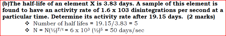
(b)The half-life of an element X is 3.83 days. A sample of this element is found to have an activity rate of 1.6 x 10^3 disintegrations per second at a particular time. Determine its activity rate after 19.15 days. (c) State what is meant by an extrinsic semiconductor. (d)Figure 11, shows a depletion layer in an unbiased p-n junction 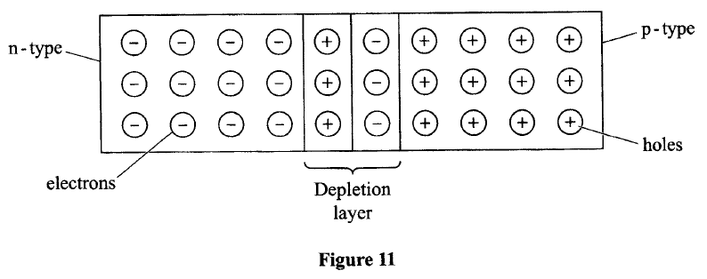
State how a battery can be used to make the depletion layer narrower.
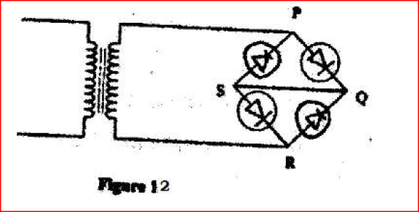
(e)Figure 12, shows an incomplete circuit of a full wave rectifier. 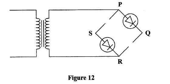
(i) Draw in the figure two more diodes to complete the circuit should be obtained.
answers
(a)Alpha radiation. This radiation has a short range with intense ionization hence thick tracks
(c)It is a semiconductor in which impurities have been added to change conductivity
(d) By connecting it in a forward biased mode
(ii)Across QS
K.C.S.E Physics Q & A - MODEL 2016PP2QN12
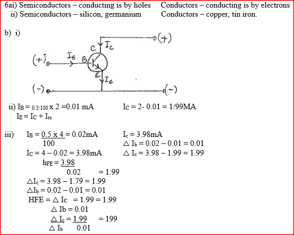
.When germanium crystal is doped with arsenic, it becomes an N-type semiconductor. Explain how this change occurs.
(Number of electrons in the outermost shell for germanium =4, arsenic =5)
answer
K.C.S.E Physics Q & A - MODEL 2015PP2QN13
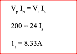
When a transformer is connected to an ac source, the output voltage is found to be 24 V. If the power input is 200 W, determine the output current. (Assume the transformer is 100% efficient)
answer
K.C.S.E Physics Q & A - MODEL 2014PP2QN08
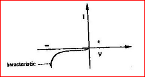
Figure 5 shows a graph of current against voltage for a semiconductor diode.
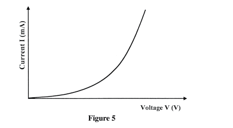
In the space provided, draw a circuit diagram that may be used to obtain values needed to draw the graph in figure 5.
answer
K.C.S.E Physics Q & A - MODEL 2013PP2QN13
When a germanium crystal is doped with arsenic, it becomes an N-type semiconductor. Explain how this change occurs.
(Number of electrons in the outermost shell for germanium = 4. Arsenic = 5)
answer
K.C.S.E Physics Q & A - MODEL 2011PP2QN19
(a) When a radiation was released into a diffusion cloud chamber, short thick tracks were observed. State with a reason, the type of radiation that was detected.
(b) The half-life of an element X is 3.83 days. A sample of this element is found to have an activity rate of 1.6 x 10³ disintegrations per second at a particular time. Determine its activity rate after 19.15 days. (c) State what is meant by an extrinsic semiconductor. (d) Figure 12, shows a depletion layer in an unbiased p-n junction. 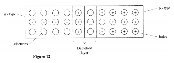
State how a battery can be used to make the depletion layer narrower.
(e) Figure 13, shows an incomplete circuit of a full wave rectifier 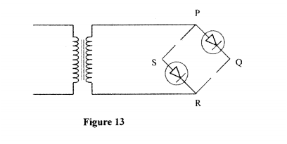
(I) Draw in the figure two more diodes to complete the circuit.
(ii) Show on the figure the points across which the output of the rectifier should obtained.
answers
(c) A semiconductor in which impurities have been added to change conductivity.
(d) By connecting it in forward biased mode (i.e. P to + and n to -) 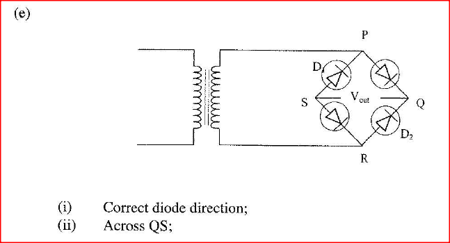
K.C.S.E Physics Q & A - MODEL 2010PP2QN14
Figure 7, shows a block diagram of a p-n junction diode.
On the same diagram. show how a battery may be connected so that the diode is reverse biased.
answer
K.C.S.E Physics Q & A - MODEL 2009PP2QN13
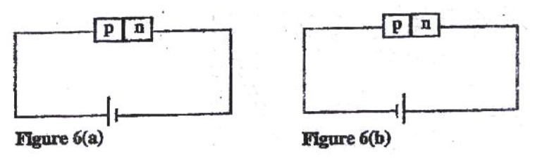
Figure 6 (a) and figure 6 (b) show a p-n junction to a battery. It is observed that the current in figure 6 (a) is greater than the current in figure 6 (b)
answer
K.C.S.E Physics Q & A - MODEL 2007PP2QN14
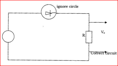
You are provided with a diode, a resistor R, an a.c source of low voltage and connecting wires.
In the space provided, sketch the circuit diagram for a half – wave rectifier and indicate the terminals where the output voltage V0 may be connected.
answer
K.C.S.E Physics Q & A - MODEL 2006PP2QN16
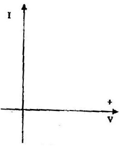
In the axes provided sketch the current – voltage characteristics for reverse – biased p- n junction
answer
K.C.S.E Physics Q & A - MODEL 2005PP2QN04
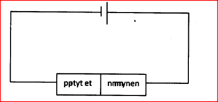
Explain how doping producers an n-type semi-conductor for a pure semi-conductor material.
b) Fig 5. Shows the circuit of a rectifier using four diodes D1, D2, D3 and d4. 
(i) Explain how a rectified output is produced from the set – up when an a.c input is connected across AB
(ii) On the axis provided sketch the graph of output voltage against time for rectifier (iii) A capacitor is now connected across XY. Explain the effect of the capacity on the output. (c) A transistor in a common-emitter amplifier has life = 120. A signal in the input causes the base corresponding change in the output voltage if the load resistance is 100n.
answers

K.C.S.E Physics Q & A - MODEL 2005PP1QN35
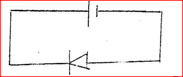
Draw appropriate symbols the circuit diagram of a junction diode in reverse bias.
ANSWER
K.C.S.E Physics Q & A - MODEL 2004PP1QN35&36
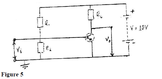
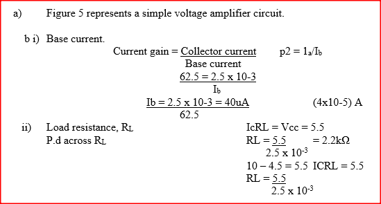
Figure 18 shows the circuit of a npn-n transistor amplifier in common –emitter mode. Use the information on the figure to answer question 35 and 36
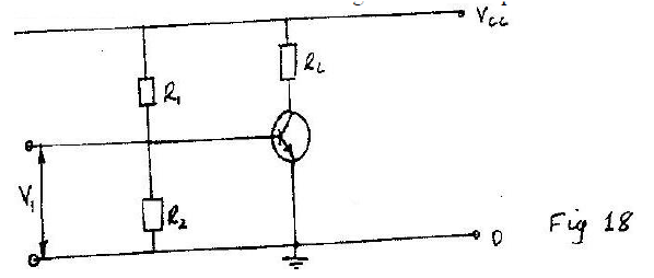
On the diagram
a) Label the collector current, Ic and IB b) Indicate the directions of 1c and 1B you have labeled in (a) above. Indicate on the diagram, the position where the output V0 would be tapped.
answer
K.C.S.E Physics Q & A - MODEL 2004PP1QN34The work function of a certain material is 3.2 3V. Determine the threshold frequency for the material. (1 electron Volt (eV)= 1.6 x10⁻¹⁹) and planks Constant h=6.62 x 10⁻³⁴Js)
answer

K.C.S.E Physics Q & A - MODEL 2003PP1QN19
Pure silicon can be changed into p –type semiconductor by adding an impurity. Explain how this is achieved.
answer
K.C.S.E Physics Q & A - MODEL 2001PP2QN05
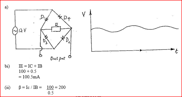
a) You are provided with 12V a.c source, four diodes and resistor.
i) Draw a circuit diagram for a full wave rectifier and show the points at which the output is taken. AC source shown-symbols; arrangement of diode (one for each pair); correct position of R; correct position of output. ii) Sketch the graph of the output when a capacitor is put in parallel with the resistor in the circuit in (i) above. 
b) A certain transistor is connected in common-emitter-mode. The base current IB is 0.50 ma. Determine the values of the:
(i) Emitter current IE. (ii) Base-collector current gain beta (iii) Current gain alpha
answers
K.C.S.E Physics Q & A - MODEL 2000PP2QN07
(a) Explain how a p- type semiconductor is made from a pure a semiconductor
(b) The curves in fig 10. Show the output characteristics of a n – p-n transistor in common emitter mode. The p.d of the battery, Vcc is 9.0V and the load resistors RL is 1.8 kohms 
i. Draw the circuit diagram for the experiment set- up that may be used to obtain the curves in the figure.
ii. Given that ohm's law for the circuit is VCE = Vcc – IcRL, draw on the same axes, the load line for the circuit ( hint: load - line passes through. (VCE = 0 and Ic = 0) Drawing load line on graph (see graph) When IB = 30μA, An alternating signal is fed into the base so that the base current changes by ± 20μA. Use the graph to determine the corresponding change in collector current Ic and hence determine the current gain beta
answers

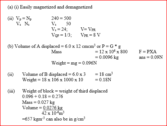
K.C.S.E Physics Q & A - MODEL 2000PP2QN04(a) (i) State one property of soft iron that makes it suitable for use as a transformer core.
|
CATEGORIES
Categories
All
Topics
FORM I - PHYSICS SYLLABUSFORM II - PHYSICS SYLLABUSTOPICS
FORM III - PHYSICS SYLLABUSFORM IV - PHYSICS SYLLABUSARCHIVES
RSS FEEDS
AUTHOR
M.A NyamotiMy passion is to see students pass using right methods and locally available resources. My emphasis is STEM courses
|
 RSS Feed