K.C.S.E Physics Q & A - MODEL 2018PP2QN18
(a) (i) Draw a circuit diagram showing the depletion layer of a p—n junction diode connected in the reverse bias mode.
(ii) State the reason why increasing the external voltage in (i) makes the depletion layer wider. (iii) State the meaning of breakdown voltage of a junction diode. (iv) State one application of diodes. (b) Figure 7 shows the output on a screen of a CR0 when an a.c. signal is connected to the Y-plates with the time base on. 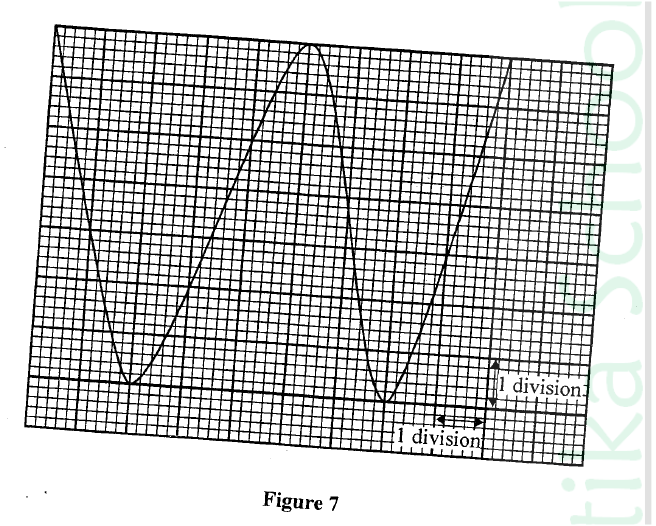
(i) Given that the time control is 5 ms per division and the y-gain is 100 V per division determine the:
(I) frequency of the ac. signal (II) peak voltage of the input signal (ii) State the adjustment that may be made in order to halve the frequency of the a.c. signal.
answers
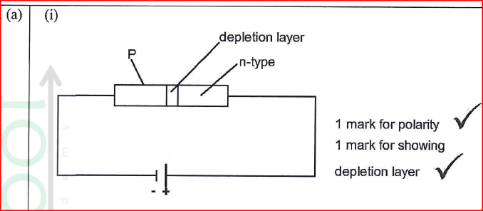
(ii) The holes and the electrons in their respective regions are attracted away from the junction by the external voltage.
(iii) The voltage at which the diode begins to conduct in the reverse bias mode. (iv) In rectification circuits for changing a.c. to d. c. In control of voltages of Zener diode. 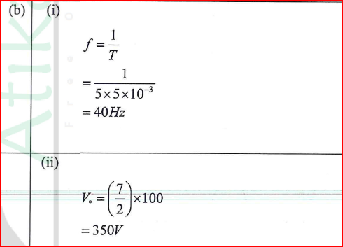
(iii) Double the time control to 10ms per division.
Adjust the frequency of the source to half the value
0 Comments
Leave a Reply. |
CATEGORIES
Categories
All
Topics
FORM I - PHYSICS SYLLABUSFORM II - PHYSICS SYLLABUSTOPICS
FORM III - PHYSICS SYLLABUSFORM IV - PHYSICS SYLLABUSARCHIVES
RSS FEEDS
AUTHOR
M.A NyamotiMy passion is to see students pass using right methods and locally available resources. My emphasis is STEM courses
|
 RSS Feed